Coworker Tony DeRose wrote up his experience in fabbing his own PCBs, and has graciously allowed me to post them here. Check out his drain cleaner comment in step 7 and you'll know why he's such a great guy to work with!
I've finally started to look into making my own 1 and 2 layer pcbs. I've experimented with a few inexpensive methods. Here's a description of the best I've found so far. Let me know if you have a better process.
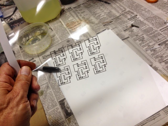
Step 1: Laser print the layout on transparency film (costs 80 cents at Kinko's). Layout was created in Eagle (lite).
Step 2: Buy pretreated photosensitive pcb board. About $7 for this size at Lasher's.
Step 3: Cut a piece from the board to size.
Step 4: Using a "safelight" that won't expose the board (a 40W incandescent bulb), peel off the protective white layer.
Step 5: Lay the pattern on the board (treated side up) and cover with an acrylic plate to hold it in place.
Step 6: Expose under a photo lamp for 5-8 minutes.
Step 7: UV light makes the exposed parts of the board susceptible to removal using NaOH solution. Place in a NaOH bath until the pattern becomes clearly visible. In my experiment last night this took about 30 seconds. Immediately rinse in a water bath to remove excess NaOH. The bottle says 1 part concentrated solution to 7 parts water. I got better results with a ration of 1:10 using the product below. I think you can go even cheaper and use drain cleaner, but I haven't tried that yet.
Step 8: Etch away the copper using equal parts 14% HCL and 3% H2O2. OSH carries the HCL as a pool chemical (also called muriatic acid). Any drug store has peroxide. Takes about 10 mins.
Step 9: Rinse in water and dry.
blogodex = {"idx" : ["PCB", "Board Etching", "Tony DeRose"]};


No comments:
Post a Comment